 Contact
 Intranet
 SK
SK


Transition Metal Dichalcogenides (TMDs) are a group of materials with the general formula MX2, where M is a transition metal from groups IV (e.g., Ti, Zr, Hf, etc.), V (e.g., V, Nb, Ta), or VI (Mo, W) of the periodic table, and X is a chalcogen (S, Se, or Te). The crystal structure of TMD materials consists of weakly bound layers of X-M-X, where the metal layer is enclosed between two layers of X, with atoms in the layer bound hexagonally. Adjacent layers are weakly bonded through van der Waals interactions, allowing the preparation of these materials in the form of single or few layers. There are more than 40 combinations of transition metals and chalcogens, with individual compounds differing in their properties. For example, NiTe2 and VSe2 are semimetals, MoS2, WS2, WSe2, MoSe2, MoTe2, TaS2, RhTe2, PdTe2 are semiconductors, HfS2 is an insulator, NbS2, NbSe2, NbTe2, and TaSe2 are superconductors; Bi2Se3, Bi2Te3 can be topological insulators, and TiSe2 exhibits CDW (charge density wave) and superconducting ground states.
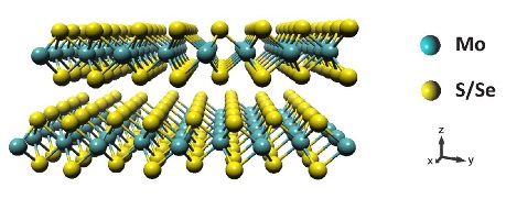
Figure 1 Three-dimensional schematic representation of the MoS/Se2 structure, with chalcogen atoms (X) in yellow and metal atoms (Mo) in blue.
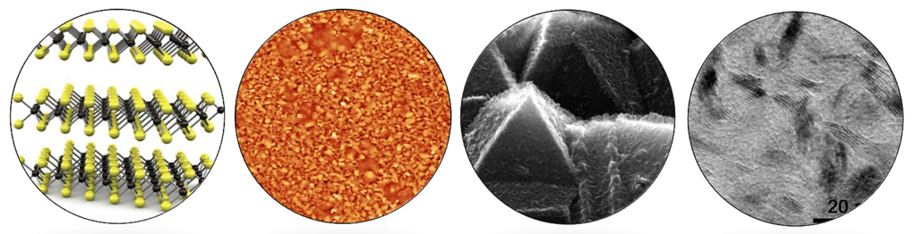
In our department, we prepare some layers of TMD materials using chalcogenization (sulfurization, selenization) of metal layers. This method is commonly used for TMD preparation, but we have designed and are currently using its modified variant (Figure 2). In the conventional process, the chalcogen slowly evaporates in the cooler zone of a two-zone furnace, while the substrate with the thin metal layer is located in another zone with a much higher temperature. In our chalcogenization method, a one-zone furnace with the sample placed in the center of the furnace together with chalcogen powder is sufficient. The sample and chalcogen powder have the same temperature. Using this approach, we have prepared ultrathin layers and large-area layers (up to 20 × 20 mm2) of several TMD materials: MoS2, PtSe2, MoSe2, WS2, and PtS2.
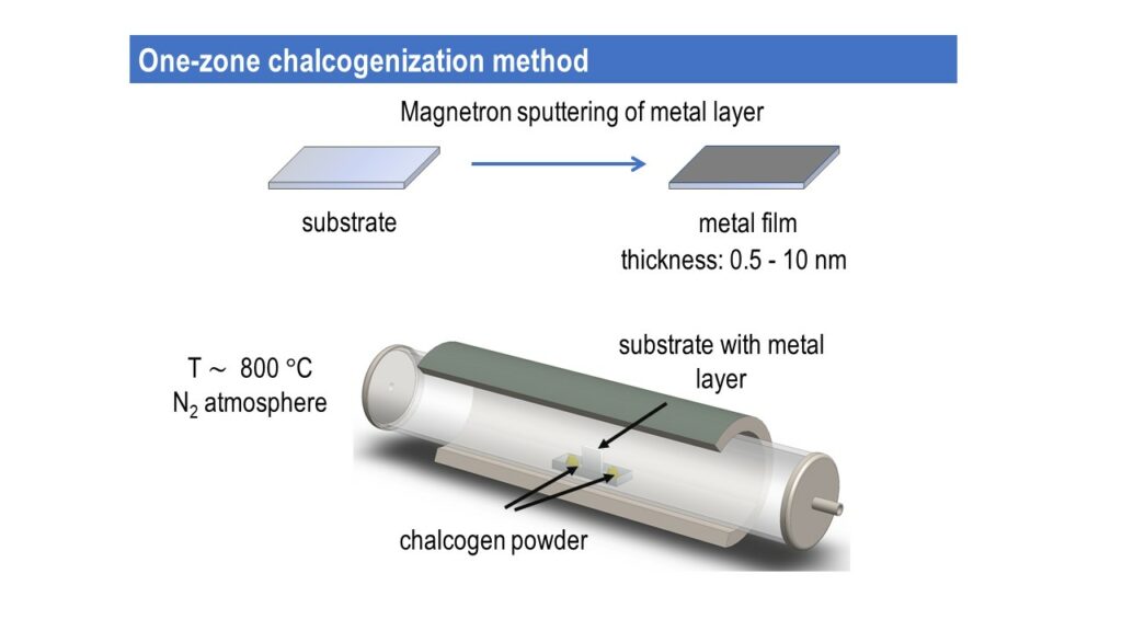
Figure 2 Schematic representation of one-zone chalcogenization.
Molybdenum disulfide (MoS2) is the most widely used material from this group. Due to its characteristic properties, it is used in various areas, such as catalysis in the petrochemical industry, photovoltaic cells, nanotribology, lithium batteries, or as a dry lubricant. In the preparation of MoS2, we can deliberately influence the orientation of the layers by changing the annealing parameters and prepare MoS2 with horizontal or vertical orientation. Figure 2 shows GIWAXS reciprocal space maps of MoS2 layers with different orientations. We have also succeeded in preparing thin MoS2 layers on gallium phosphide nano-cones and diamond substrates for the first time.
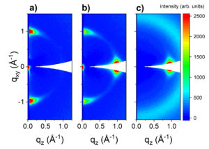
Figure 3 GIWAXS reciprocal space maps of MoS2 layers prepared on a sapphire substrate from 3 nm thick Mo layers at 800 °C for 30 minutes with heating rates (a) 25 °C/min, (b) 5 °C/min, and (c) 0.5 °C/min. Peaks at -1 A-1 originate from (002) diffraction planes.
Platinum diselenide (PtSe2) has shown promise as a material for studying quasi-particle interactions and developing photoelectric devices. Monolayer and few-layer PtSe2 are p-type semiconductors, but thicker PtSe2 exhibits typical semimetallic characteristics. Due to its electrical properties and excellent air stability, PtSe2 has potential in various areas, such as photocatalysis, hydrogen evolution, electronic, and optoelectronic devices. Recently, we have prepared highly crystalline PtSe2 layers with epitaxial character, meaning that the layers follow the crystallographic orientation of the substrate (Figure 4). The samples are highly conductive and exhibit good charge carrier mobility. Thin PtSe2 layers have also been prepared on the surface of superconducting NbN. We found that selenization parameters maintain the chemical and structural integrity of PtSe2 and NbN films. The orientation of PtSe2 can be influenced by changing the nitrogen flow rate through the reaction chamber. The integration of semiconductors and transistor gain elements with NbN-based superconductors opens up several new opportunities, such as single-photon detectors integrated with HEMT amplifiers for secure quantum communications or HEMT microwave amplifiers with superconducting Josephson junctions, providing a platform for superconducting qubits.
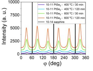
Figure 4 Phi-scan of the 101 diffraction of PtSe2 layers prepared at 400 and 600 °C on a sapphire substrate.
Selected publications:
Sojková, M., Píš, I., Hrdá, J., Vojteková, T., Pribusová Slušná, L., Vegso, K., Šiffalovič, P., Nádaždy, P., Dobročka, E., Krbal, M., Fons, P.J., Munnik, F., Magnano, E., Hulman, M., and Bondino, F.: Lithium-induced reorientation of few-layer MoS2 films, Chem. Mater. 35 (2023) 6246-6257.
Kočí, M., Izsák, T., Vanko, G., Sojková, M., Hrdá, J., Szabó, O., Husák, M., Végsö, K., Varga, M., and Kromka, A.: Improved gas sensing capabilities of MoS2/diamond heterostructures at room temperature, ACS Applied Mater. Interfaces 15 (2023) 34206-34214.
Varga, M., Sojková, M., Hrdá, J., Parza Saeb, S., Vanko, G., Pribusová-Slušná, L., Ondic, L., Fait, J., Kromka, A., and Hulman, M.: Technological challenges in the fabrication of MoS2/diamond heterostructures. In NANOCON 2022. Proc. 14th Inter. Conf. Nanomater. – Res. & Appl. Ostrava. Tanger Ltd. 2023, pp 21-27. ISBN: 978-80-88365-09-9.
Vegso, K., Shaji, A., Sojková, M., Pribusová Slušná, L., Vojteková, T., Hrdá, J., Halahovets, Y., Hulman, M., Jergel, M., Majková, E., Wiesmann, J., and Šiffalovič, P.: A wide-angle X-ray scattering laboratory setup for tracking phase changes of thin films in a chemical vapor deposition chamber, Rev. Sci Instrum. 93 (2022) 113909.
Shaji, A., Vegso, K., Sojková, M., Hulman, M., Nádaždy, P., Halahovets, Y., Pribusová Slušná, L., Vojteková, T., Hrdá, J., Jergel, M., Majková, E., Wiesmann, J., and Šiffalovič, P.: Stepwise sulfurization of MoO3 to MoS2 thin films studied by real-time X-ray scattering, Applied Surface Sci 606 (2022) 154772.
Kozak, A., Sojková, M., Gucmann, F., Bodík, M., Vegso, K., Dobročka, E., Píš, I., Bondino, F., Hulman, M., Šiffalovič, P., and Ťapajna, M.: Effect of the crystallographic c-axis orientation on the tribological properties of the few-layer PtSe2, Applied Surface Sci 605 (2022) 154883.
Novák, J., Laurenčíková, A., Eliáš, P., Hasenöhrl, S., Sojková, M., Kováč, J.jr., and Kováč, J.: Investigation of a nanostructured GaP/MoS2 p-n heterojunction photodiode, AIP Adv. 12 (2022) 065004.
Sojková, M., Hrdá, J., Volkov, S., Vegso, K., Shaji, A., Vojteková, T., Pribusová Slušná, L., Gál, N., Dobročka, E., Šiffalovič, P., Roch, T., Gregor, M., and Hulman, M.: Growth of PtSe2 few-layer films on NbN superconducting substrate, Applied Phys. Lett. 119 (2021) 013101.
Pribusová Slušná, L., Vojteková, T., Hrdá, J., Pálková, H., Šiffalovič, P., Sojková, M., Vegso, K., Hutár, P., Dobročka, E., Varga, M., and Hulman, M.: Optical characterisation of few-layer PtSe2 nanosheet films, ACS Omega 6 (2021) 35398-35403.
Hrdá, J., Tašková, V., Vojteková, T., Pribusová Slušná, L., Dobročka, E., Píš, I., Bondino, F., Hulman, M., and Sojková, M.: Tuning the charge carrier mobility in few-layer PtSe2 films by Se: Pt ratio, RSC Adv. 11 (2021) 27292.
Huss-Hansen, M.K., Hodas, M., Mrkývkova, N., Hagara, J., Nádaždy, P., Sojková, M., Høegh, S.O., Vlad, A., Pandit, P., Majková, E., Šiffalovič, P., Schreiber, F., Kjelstrup-Hansen, J., and Knaapila, M.: Early-stage growth observations of orientation-controlled vacuum-deposited naphthyl end-capped oligothiophenes, Phys. Rev. Mater. 5 (2021) 053402.
Shaji, A., Vegso, K., Sojková, M., Hulman, M., Nádaždy, P., Hutár, P., Pribusová Slušná, L., Hrdá, J., Bodik, M., Hodas, M., Bernstorff, S., Jergel, M., Majková, E., Schreiber, F., and Šiffalovič, P.: Orientation of few-layer MoS2 films: in-situ x-ray scattering study during sulfurization, J. Phys. Chem. C 125 (2021) 9461–9468.
Mrkývkova, N., Cernescu, A., Futera, Z., Nebojsa, A., Dubroka, A., Sojková, M., Hulman, M., Majková, E., Jergel, M., Šiffalovič, P., and Schreiber, F.: Nanoimaging of orientational defects in semiconducting organic films, J. Phys. Chem. C 125 (2021) 9229–9235.
Rýger, I., Lobotka, P., Steiger, A., Chromik, Š., Lalinský, T., Raida, Z., Pítra, K., Zehetner, J., Španková, M., Gaži, Š., Sojková, M., and Vanko, G.: Uncooled antenna-coupled microbolometer for detection of terahertz radiation, J. Infrared, Millimet., Terahertz Waves 42 (2021) 462–478.
Hotový, I., Spiess, L., Mikolášek, M., Kostič, I., Sojková, M., Romanus, H., Hulman, M., Buc, D., and Řeháček, V.: Layered WS2 thin films prepared by sulfurization of sputtered W films, Applied Surface Sci 544 (2021) 148719.
Španková, M., Sojková, M., Dobročka, E., Hutár, P., Bodík, M., Munnik, F., Hulman, M., and Chromik, Š.: Influence of precursor thin-film quality on the structural properties of large-area MoS2 films grown by sulfurization of MoO3 on c-sapphire, Applied Surface Sci 540 (2021) 148240.
Sojková, M., Dobročka, E., Hutár, P., Tašková, V., Pribusová Slušná, L., Stoklas, R., Píš, I., Bondino, F., Munnik, F., and Hulman, M.: High carrier mobility epitaxially aligned PtSe2 films grown by one-zone selenization, Applied Surface Sci 538 (2021) 147936.
Bodík, M., Sojková, M., Hulman, M., Ťapajna, M., Truchlý, M., Vegso, K., Jergel, M., Majková, E., Španková, M., and Šiffalovič, P.: Friction control by engineering the crystallographic orientation of the lubricating few-layer MoS2 films, Applied Surface Sci 540 (2021) 148328.
Sojková, M., Végso, K., Mrkývkova, N., Hagara, J., Hutár, P., Rosová, A., Čaplovičová, M., Ludacka, U., Skákalová, V., Majková, E., Šiffalovič, P., and Hulman, M.: Tuning the orientation of few-layer MoS2 films using one-zone sulfurization, RSC Adv. 9 (2019) 29645-29651.
Sojková, M., Šiffalovič, P., Babchenko, O., Vanko, G., Dobročka, E., Hagara, J., Mrkývková, N., Majková, E., Ižák, T., Kromka, A., and Hulman, M.: Carbide-free one-zone sulfurization method grows thin MoS2 layers on polycrystalline CVD diamond, Sci Rep. 9 (2019) 2001.
Novák, J., Laurenčíková, A., Eliáš, P., Hasenöhrl, S., Sojková, M., Dobročka, E., Kováč, J.jr., Kováč, J., Ďurišová, J., and Pudiš, D.: Nanorods and nanocones for advanced sensor applications, Applied Surface Sci 461 (2018) 61-65.
Hotový, I., Spiess, L., Sojková, M., Kostič, I., Mikolášek, M., Predanocy, M., Romanus, H., Hulman, M., and Řeháček, V.: Structural and optical properties of WS2 prepared using sulfurization of different thick sputtered tungsten films, Applied Surface Sci 461 (2018) 133-138.
Chromik, Š., Sojková, M., Vretenár, V., Rosová, A., Dobročka, E., Hulman, M., : Influence of GaN/AlGaN/GaN (0001) and Si (100) substrates on structural properties of extremely thin MoS2 films grown by pulsed laser deposition. Applied Surface Sci 395 (2017) 232-236.
Sojková, M., Chromik, Š., Rosová, A., Dobročka, E., Hutár, P., Machajdík, D., Kobzev, A., Hulman, M., : MoS2 thin films prepared by sulfurization. Proc. SPIE 10354 (2017) 103541K-1.