 Contact
 Intranet
 SK
SK


Detection of ionizing radiation
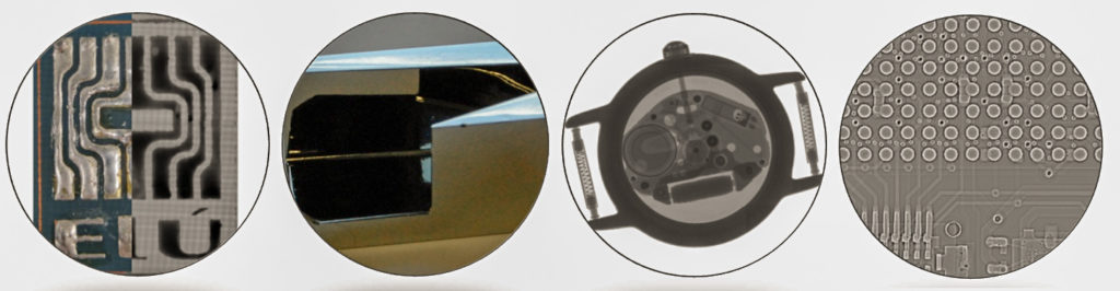
The ionizing radiation passing through the matter demonstrates various physical phenomena, which can be used for detection or measurement of its characteristics. The primary component of measurement set-up of ionizing radiation is detector or sensor. Sensitive part of the sensor is semiconductor material like silicon, gallium arsenide, cadmium teluride, indium phospide and others. According to character or ionizing radiation (alpha, beta, X-rays, g-rays and others) and its parameters which we try to detect, it is necessary to match detector parameters (like sensitive area, thickness and others). In our department we developed and tested so-called „single“ detector and also 2D pixel structures for digital radiation camera (Fig. 1). As a base detection material, we used 4H-SiC and also semiinsulating GaAs semiconductor.
a) 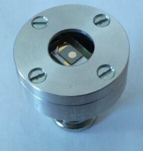 b)
b) 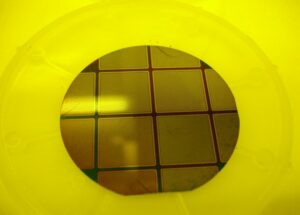
Fig. 1. a) Photograph of encapsulated „single“ detector based on 4H-SiC; b) Semiconductor substrate based on GaAs with fabricated pixel structures of 55 mm pitch.
Prepared semiconductor detectors are connected to the read-out chain processing detector signals. Sensors are able to measure the energy or ionizing radiation with high precision. Fig 2a shows detected peak of a-particles generated by radioisotope sources 239Pu, 241Am a 244Cm. The SiC sensor can operated at very high temperatures. Fig. 2b demonstrates comparison of detection properties for a-particles at room temperature and 500 °C. It is observable that optimized SiC detector has almost identical characteristics also at extremely high temperature.
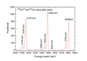
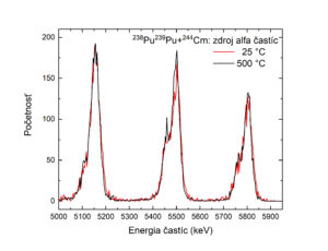
Fig. 2. a) Measured spectrum of a-particles with 4H-SiC detector; b) comparison of the spectrometric performance of 4H-SiC detector at 25 °C and 500 °C.
2D pixel detector field are important in the imaging of ionizing radiation. Base on detection track it is possible to determine type of detected particle and its energy. Fig. 3 shows tracks of various type of radiation (X-rays, electrons, a-particles) obtained by radiation camera based on GaAs sensor. Typical number of pixels in radiation camera is 256 × 256 pixels.
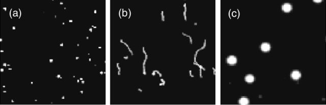
Fig. 3 a) Tracks of 60 keV X-ray photons; b) 546 keV electrons; c) 5.5 MeV a-particles.
X-ray crystal optics
X-ray crystal optics are produced from monocrystalline materials that have a precisely defined crystallographic orientation of the atomic planes. Silicon (Si) and Germanium (Ge) are most often used for hard X-rays. In combination with X-ray cameras the crystal optics can increase spatial resolution of such cameras. With the development of new, more intensive X-ray sources, such as free electron X-ray lasers (XFEL), other more heat-resistant materials such as Diamond (C) or Silicon Carbide (SiC) can be used as X-ray optical elements.
The shape of the X-ray beam and its spectral properties are adjusted using X-ray crystal optics. For example, the X-ray can be expanded or focused in one or two directions and at the same time the X-ray beam is monochromatized. Monochromatic X-rays allow to better quantitatively evaluate various measurements, whether it is X-ray metrology or X-ray imaging.
We are engaged in research and development of new types of X-ray optics with highly accurate planar and curved active surfaces. We are preparing surfaces in cooperation with an industrial partner using innovative high-precision nanomachining technology. The nanomachining method uses mechanical removal of material with a depth of cut from 0.125 to 10 micrometers using a single diamond tip tool and allows to produce surfaces with high shape accuracy, nanometer surface roughness and minimal damage to the crystal lattice in the subsurface area. We also develop procedures for chemo-mechanical and chemical polishing of curved surfaces (cylindrical, parabolic, logarithmic, …) in order to remove periodic traces of tools and areas with subsurface deformation of the crystal lattice, which are created due to the deterministic nature of nanomachining.
New elements of X-ray optics and their sets are tested in real laboratory experiments of X-ray metrology (SAXS / GISAXS, HRXRD) and X-ray imaging with microfocus X-ray sources. In cooperation with Institute of Physics of the Slovak Academy of Sciences, a high-intensity microfocus X-ray source with a liquid Ga anode and another with a fixed Cu anode are available. The ionizing radiation detectors based on Medipix technology that we develop at the IEE SAS are directly used in combination with new elements of X-ray optics in experimental sets. For highly accurate optics adjustment within the X-ray system, we use the existing laboratory infrastructure such as high-precision goniometers or hexapods with a positioning accuracy of 0.0001 mm. Depending on the allocation of machine time, we also test the optics on synchrotron radiation sources. Here we mainly use our international cooperation.
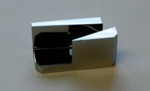
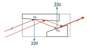
Fig. 4. A picture of an X-ray crystal optics element prepared from germanium single crystal (left-hand side) and a principle of X-ray beam compression (right-hand side).
Selected publications:
Osvald, J., Hrubčín, L., and Zaťko, B.: Temperature dependence of electrical behaviour of inhomogeneous Ni/Au/4H–SiC Schottky diodes, Mater. Sci Semicond. Process. 140 (2022) 106413.
Zaťko, B., Hrubčín, L., Šagátová, A., Osvald, J., Boháček, P., Kováčová, E., Halahovets, Y., Rozov, S.V., and Sandukovskij, V.G.: The study of Schottky barrier detectors based on high quality 4H-SiC epitaxial layer with different thickness, Applied Surface Sci 536 (2021) 147801.
Osvald, J., Hrubčín, L., and Zaťko, B.: Schottky barrier height inhomogeneity in 4H-SiC surface barrier detectors, Applied Surface Sci 533 (2020) 147389.
Dubecký, F., Zaťko, B., Kolesár, V., Kindl, D., Hubík, P., Gombia, E., and Dubecký, M.: Charge collection efficiency of Pt vs. Mg contacts on semi-insulating GaAs, Applied Surface Sci 467-468 (2019) 1219-1225.
Kubanda, D., Zaťko, B., Šagátová, A., Žemlička, J., Zápražný, Z., Boháček, P., Dudák, J., Kováčová, E., and Nečas, V.: Performance of bulk semi-insulating GaAs-based sensor and its comparison to Si-based sensor for Timepix radiation camera, J. Instrument. 14 (2019) C01023.
Šagátová, A., Zaťko, B., Dubecký, F., Ly Anh, T., Nečas, V., Sedlačková, K., Pavlovič, M., Fülöp, M., :Radiation hardness of GaAs sensors against gamma-rays, neutrons and electrons. Applied Surface Sci 395 (2017) 66-71.
Zaťko, B., Šagátová, A., Sedlačková, K., Boháček, P., Sekáčová, M., Kohout, Z., Granja, C., Nečas, V., :Radiation detector based on 4H-SiC used for thermal neutron detection. J. Instrument. 11 (2016) C11022.
Zápražný, Z., Korytár, D., Jergel, M., Šiffalovič, P., Halahovets, Y., Keckes, J., Maťko, I., Ferrari, C., Vagovič, P., Mikloška, M., : Nano-machining for advanced x-ray crystal optics. AIP Conf. Proc. 1764 (2016) 020005.
Korytár, D., Zápražný, Z., Ferrari, C., Frigeri, C., Jergel, M., Maťko, I., and Kečkeš, M.: Cross-sectional TEM study of subsurface damage in SPDT machining of germanium optics, Applied Optics 57 (2018) 1940-1943.
Zápražný, Z., Korytár, D., Jergel, M., Halahovets, Y., Kotlár, M., Maťko, I., Hagara, J., Šiffalovič, P., Keckes, J., and Majková, E.: Characterization of the chips generated by the nanomachining of germanium for X-ray crystal optics, Inter. J. Adv. Manufactur. Technol. 102 (2019) 2757-2767.
Zápražný, Z., Zaťko, B., Korytár, D., Gál,, Jergel, M., Halahovets, Y., and Ferrari, C.: Testing of thickness homogeneity of Si crystal membranes using GaAs Timepix detector, J. Instrument. 16 (2021) P06015.
Nádaždy, P., Hagara, J., Mikulík, P., Zápražný, Z., Korytár, D., Majková, E., Jergel, M., and Šiffalovič, P.: A high-throughput assembly of beam-shaping channel-cut monochromators for laboratory high-resolution X-ray diffraction and small-angle X-ray scattering experiments, J. Applied Crystall. 54 (2021) 730-738.