 Contact
 Intranet
 SK
SK


People | Publications | Back
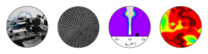
Graphene and graphene oxide
Graphene was discovered in 2004 by a group of researchers led by Andre Geim and Konstantin
Novoselov at the University of Manchester. This is a two-dimensional material where carbon atoms are
arranged in a hexagonal structure like honeycomb. Graphene has a thickness of only one monolayer (~
0.34 nanometre) and is chemically stable under normal conditions in air.
Many graphene layers arranged on top of each other according to a certain pattern create a crystal of
graphite. Scientists used graphene as a model for the calculation and determination of the properties of
graphite for decades. But no one foresaw that the layer a single atom thick was also really stable.
Therefore, mere discovery of graphene has attracted considerable acclaim in the scientific community.
The curious way the first samples were prepared also contributed to that. It was a mechanical method of
exfoliation of layers of a graphite crystal. And for that, a scotch tape, substrate and a lot of patience was
enough.
Currently, chemical vapour deposition is one of the most widely used method for preparation of
graphene. A gas which contains carbon (e.g. methane) is to decompose at high temperatures in contact
with certain metals which act as a catalyst (e.g. copper). Free carbon atoms are arranged on the surface
of the metal to the hexagonal graphene lattice. After copper is dissolved, a graphene layer can be
transferred to any substrate as desired. Many “exotic” physical phenomena have been observed in
graphene such as Klein’s paradox, existence of massless particles with high mobility, quantum Hall
effect at room temperature and others.
Studies of electrical transport characteristics of graphene have revealed its great potential for electronics.
Operating frequency of transistors made of graphene in the gigahertz region can overcome the speed of
most modern computers in the near future. Important applications of graphene are foreseen for chemical
sensors that use extremely sensitive changes in conductivity when exposed to various chemical
adsorbants. The unique combination of high optical transparency and a large conductivity of graphene
layers can be used in a wide range of optoelectronic components such as displays or solar cells.
Another way to prepare graphene is chemical oxidation of graphite powders. Molecules containing
oxygen intercalate the graphite layers and bind chemically to them. This process causes the inter-layer
distance to increase to the point when a layer is exfoliated from the parent crystal. It is actually a
chemical analogue of the original method of mechanical exfoliation. This way, monoatomic layers with
lateral dimensions of the order of hundreds of nanometres to micrometres are obtained. The layers are
strongly oxidized, so in this case we are talking about graphene oxide.
An interesting feature of graphene oxide (GO) is that the level of its oxidation can be varied by reducing
the concentration of oxygen molecules either chemically or by thermal annealing. Changing the
concentration of oxide has a significant impact on the electrical transport properties of reduced GO
(rGO). In terms of electrical conductivity, fully oxidized graphene behaves as an insulator. The reduction
increases the conductivity in many orders of magnitude, and completely reduced GO has properties
similar to those of graphene.
The combination of a porous structure (high surface area) and a relatively high conductivity of rGO
implies the use of this material for some applications. Electrodes made of rGO in supercapacitors is one
of such examples.
Recent publications:
Hrdá, J., Tašková, V., Vojteková, T., Pribusová Slušná, L., Dobročka, E., Píš, I., Bondino, F., Hulman, M., and Sojková, M.: Tuning the charge carrier mobility in few-layer PtSe2 films by Se: Pt ratio, RSC Adv. 11 (2021) 27292. (APVV 17-0352, 17-0560, 19-0365, VEGA 2/0059/21, CEMEA ITMS 313021T081)
Hrdá, J., Tašková, V., Vojteková, T., Pribusová Slušná, L., Dobročka, E., Píš, I.. Bondino, F., Hulman, M., and Sojková, M.: Selenium content influences the charge carrier mobility in few-layer PtSe2 films. In Proc. 9th Inter. Conf. on Advances in Electron. Photon. Technol. – ADEPT. Žilina: EDIS 2021. ISBN 978-80-554-1735-6. P. 103-106.
Hulman, M.: Raman spectroscopy of graphene. In Graphene: properties, preparation, characterization, and applications. Elsevier 2021, p. 381-412. ISBN 978-0-08-102848-3.
Pribusová Slušná, L., Vojteková, T., Hrdá, J., Pálková, H., Šiffalovič, P., Sojková, M., Vegso, K., Hutár, P., Dobročka, E., Varga, M., and Hulman, M.: Optical characterisation of few-layer PtSe2 nanosheet films, ACS Omega 6 (2021) 35398-35403. (APVV 15-0693, 19-0365, 20-0111, VEGA 2/0059/21, MoRePro 19MRP0010)
Sojková, M., Hrdá, J., Volkov, S., Vegso, K., Shaji, A., Vojteková, T., Pribusová Slušná, L., Gál, N., Dobročka, E., Šiffalovič, P., Roch, T., Gregor, M., and Hulman, M.: Growth of PtSe2 few-layer films on NbN superconducting substrate, Applied Phys. Lett. 119 (2021) 013101. ( APVV 15-0693, 17-0352, 297, 17-0560, 19-0365, VEGA 2/0149/17, 2/0059/21, CEMEA ERDF ITMS 313021T081)
Bodík, M., Sojková, M., Hulman, M., Ťapajna, M., Truchlý, M., Vegso, K., Jergel, M., Majková, E., Španková, M., and Šiffalovič, P.: Friction control by engineering the crystallographic orientation of the lubricating few-layer MoS2 films, Applied Surface Sci 540 (2021) 148328. (APVV-15-0693, 17-0352, 17-0560, SK-CN-RD-18-0006, 14-0745, VEGA 2/0149/17, 2/0092/18)
Sojková, M., Dobročka, E., Hutár, P., Tašková, V., Pribusová Slušná, L., Stoklas, R., Píš, I., Bondino, F., Munnik, F., and Hulman, M.: High carrier mobility epitaxially aligned PtSe2 films grown by one-zone selenization, Applied Surface Sci 538 (2021) 147936.
Hotový, I., Spiess, L., Mikolášek, M., Kostič, I., Sojková, M., Romanus, H., Hulman, M., Buc, D., and Řeháček, V.: Layered WS2 thin films prepared by sulfurization of sputtered W films, Applied Surface Sci 544 (2021) 148719. (VEGA 1/0529/20, APVV-16-0266, 17-0169)
Shaji, A., Vegso, K., Sojková, M., Hulman, M., Nádaždy, P., Hutár, P., Pribusová Slušná, L., Hrdá, J., Bodik, M., Hodas, M., Bernstorff, S., Jergel, M., Majková, E., Schreiber, F., and Šiffalovič, P.: Orientation of few-layer MoS2 films: in-situ x-ray scattering study during sulfurization, J. Phys. Chem. C 125 (2021) 9461–9468.
Mrkývkova, N., Cernescu, A., Futera, Z., Nebojsa, A., Dubroka, A., Sojková, M., Hulman, M., Majková, E., Jergel, M., Šiffalovič, P., and Schreiber, F.: Nanoimaging of orientational defects in semiconducting organic films, J. Phys. Chem. C 125 (2021) 9229–9235.
Sojková, M., Hrdá, J., Volkov, S., Végso, K., Shaji, A., Vojteková, T., Pribusová Slušná, L., Gál, N., Dobročka, E., Šiffalovič, P., Roch, T., Gregor, M., and Hulman, M.: PtSe2 few-layer films grown on NbN superconducting substrate. In Proc. 9th Inter. Conf. on Advances in Electron. Photon. Technol. – ADEPT. Žilina: EDIS 2021. ISBN 978-80-554-1735-6. P. 9-12.
Hutár, P., Sojková, M., Kundrata, I., Vegso, K., Shaji, A., Nádaždy, P., Pribusová Slušná, L., Majková, E., Siffalovic, P., and Hulman, M.: Correlation between the crystalline phase of molybdenum oxide and horizontal alignment in thin MoS2 films, J. Phys. Chem. C 124 (2020) 19362–19367. (APVV-15-0693, 17-0352, 17-0560, 19-0365, VEGA 2/0149/17, ITMS project code 313021T081)
Hagara, J., Mrkývkova, N., Nádaždy, P., Hodas, M., Bodík, M., Jergel, M., Majková, E., Tokár, K., Hutár, P., Sojková, M., Chumakov, A., Konovalov, O., Pandit, P., Roth, S., Hinderhofer, A., Hulman, M., Šiffalovič, P., and Schreiber, F.: Reorientation of π-conjugated molecules on few-layer MoS2 films, Phys. Chem. Chem. Phys. 22 (2020) 3097-3104. (APVV 17-0352, 16-0319, 15-0641, 15-0693, 14-0745, SK-CN-RD-18-0006; VEGA 2/0092/18, 2/0149/17; ITMS 26230120002, 26210120002, 313021T081; DAAD/SAV)
Hagara, J., Mrkývkova, N., Feriancová, L., Putala, M., Nádaždy, P., Hodas, M., Shaji, A., Nádaždy, V., Huss-Hansen, M.K., Knaapila, M., Hagenlocher, J., Russegger, N., Zwadlo, M., Merten, L., Sojková, M., Hulman, M., Vlad, A., Pandit, P., Roth, S., Jergel, M., Majková, E., Hinderhofer, A., Šiffalovič, P., and Schreiber, F.: Novel highly substituted thiophene-based n-type organic semiconductor: structural study, optical anisotropy and molecular control, CrystEngComm 22 (2020) 7095-7103. (APVV-19-0365, 18-0480, 17-0352, 17-0560, 17-0501, 16-0319, 15-0641, 15-0693, 14-0745, SK-CNRD-18-0006, VEGA 2/0092/18, 2/0149/17, 1/0595/17, ITMS 26210120023, 26230120002, 26210120002, 26220220170, 313021T081, DAAD/SAV grant)
Mrkývkova, N., Nádaždy, P., Hodas, M., Chai, J., Wang, S., Chi, D., Sojková, M., Hulman, M., Chumakov, A., Konovalov, O.V., Hinderhofer, A., Jergel, M., Majková, E., Šiffalovič, P., and Schreiber, F.: Simultaneous monitoring of molecular thin film morphology and crystal structure by x-ray scattering, Cryst. Growth Des. 20 (2020) 5269–5276.
Sojková, M., Dobročka, E., Hutár, P., Tašková, V., Pribusová Slušná, L., Stoklas, R., Píš, I., Bondino, F., Hulman, M., and Gregušová, D.: Epitaxially aligned PtSe2 films grown by one-zone selenization. In Proc. 8th Inter. Conf. on Advances in Electron. Photon. Technol. – ADEPT. Žilina: EDIS 2020. ISBN 978-80-554-1735-6. P. 6-9.
Brndiarová, J., Šiffalovič, P., Hulman, M., Kalosi, A., Bodik, M., Skákalová, V., Micusik, M., Markovič, Z., Majková, E., and Fröhlich, K.: Functionalized graphene transistor for ultrasensitive detection of carbon quantum dots, J. Applied Phys. 126 (2019) 214303. (APVV 15-0641, 15-0693, VEGA 2/0136/18)
Hutár, P., Španková, M., Sojková, M., Dobročka, E., Végso, K., Hagara, J., Halahovets, Y., Majková, E., Šiffalovič, P., and Hulman, M.: Highly crystalline MoS2 thin films fabricated by sulfurization, Phys. Status Solidi B 256 (2019) 1900342. (APVV 15-0693, 17-0352, 17-0560, VEGA 2/0149/17)
Sojková, M., Végso, K., Mrkývkova, N., Hagara, J., Hutár, P., Rosová, A., Čaplovičová, M., Ludacka, U., Skákalová, V., Majková, E., Šiffalovič, P., and Hulman, M.: Tuning the orientation of few-layer MoS2 films using one-zone sulfurization, RSC Adv. 9 (2019) 29645-29651. (APVV 15-0693, 15-0641, 16-0319, 17-0352, 17-0560 VEGA 2/0149/17)
Sojková, M., Šiffalovič, P., Babchenko, O., Vanko, G., Dobročka, E., Hagara, J., Mrkývková, N., Majková, E., Ižák, T., Kromka, A., and Hulman, M.: Carbide-free one-zone sulfurization method grows thin MoS2 layers on polycrystalline CVD diamond, Sci Rep. 9 (2019) 2001. (APVV 15-0693, 15-0641, 16-0319, 17-0352, VEGA 2/0149/17, P108/12/G108, SASPRO 0068/01/01)
Sojková, M., Šiffalovič, P., Babchenko, O., Vanko, G., Dobročka, E., Hagara, J., Mrkývková, N., Majková, E., Ižák, T., Kromka, A., and Hulman, M.: Carbide-free one-zone sulfurization method grown thin MOS2 layers on polycrystalline CVD diamond. In Proc. ADEPT. 7th Inter. Conf. on Advances in Electron. Photon. Technol. Žilina: Univ. Žilina 2019. ISBN 978-80-554-1568-0. P. 281-284. (APVV 15-0693, 17-0352, VEGA 2/0149/17)
Hulman, M., Sojková, M., Végso, K., Mrkývkova, N., Hagara, J., Hutár, P., Kotrusz, P., Hudec, J., Tokar, K., Majková, E., and Šiffalovič, P.: Polarized Raman reveals alignment of few-layer MoS2 films, J. Phys. Chem. C 123 (2019) 29468-29475. (APVV 17-0352, 17-0560)
Hotový, I., Spiess, L., Sojková, M., Kostič, I., Mikolášek, M., Predanocy, M., Romanus, H., Hulman, M., and Řeháček, V.: Structural and optical properties of WS2 prepared using sulfurization of different thick sputtered tungsten films, Applied Surface Sci 461 (2018) 133-138.
Skákalová, V., Kotrusz, P., Jergel, M., Susi, T., Mittelberger, A., Vretenár, V., Šiffalovič, P., Kotakoski, J., Meyer, J.C., and Hulman, M.: Chemical oxidation of graphite: evolution of the structure and properties, J. Phys. Chem. C 122 (2018) 929−935.
Janke, D., Hulman, M., Wenisch, R., Gemming, S., Rafaja, D., and Krause, M.: Influence of nickel catalyst morphology on layer-exchange-based carbon crystallisation of Ni/a-C bilayers, Phys. Status Solidi B 254 (2017) 1700234.
Susi, T., Skákalová, V., Mittelberger, A., Kotrusz, P., Hulman, M., Pennycook, T., Mangler, C., Kotakoski, J., Meyer, J., : Computational insights and the observation of SiC nanograin assembly: towards 2D silicon carbide. Sci Reports 7 (2017) 4399. (Not IEE SAS).