 Contact
 Intranet
 SK
SK


People | Publications | Back
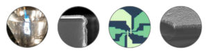
Growth of thin oxide films using atomic layer deposition technology
Atomic layer deposition (ALD) is chemical method of thin films preparation. Mostly oxide
films are prepared using this technique. ALD is based on repetition of sequence of
technological steps, when a sub-atomic oxide layer is deposited. The process takes place at
low temperatures and is characterized by high reproducibility and homogeneous growth over
large substrates, including conformal growth on 3D surfaces. At the Institute of Electrical
Engineering SAS we are able to prepare using ALD thin films of Al2O3, TiO2, HfO2, and
ZrO2.
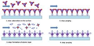
Atomic layer deposition consists of four steps:
1. Introduction of precursors, adsorption of monomolecular layer on the substrate
surface.
2. Purging of the reactor by inert gas, removal of superfluous precursor molecules.
3. Introduction of reactant gas followed by surface reaction to produce mono atomic
layer.
4. Purging of the reactor by inert gas, removal of reaction by-products.
Nowadays ALD is employed in semiconductor industry for preparation of CMOS transistors
gates and micro-capacitors for DRAM memories. In research ALD is used particularly for
preparation of thin films for resistive switching, passivation and insulation of GaN and GaAs
transistors gates and solar cells as well as for ZnO-based thin films transistor etc.
Recent publications:
Mikolášek, M., Fröhlich, K., Hušeková, K., Ondrejka, P., Chymo, F., Kemeny, M., Hotový, I., and Harmatha, L.: Development and characterisation of photoelectrochemical MIS structures with RuO2/TiO2 gate stacs for water oxidation, J. Electr. Engn. 72 (2021) 203–207. (VEGA 1/0529/20, 1/0789/21, APVV 17-0169).
Chymo, F., Fröhlich, K., Hušeková, K., Weis, M., and Mikolášek, M.: Characterization of MIS photoanodes with thin Pt layer for water splitting applications. In Proc. 9th Inter. Conf. on Advances in Electron. Photon. Technol. – ADEPT. Žilina: EDIS 2021. ISBN 978-80-554-1735-6. P. 207-210.
Sahoo, P.P., Mikolášek, M., Hušeková, K., Dobročka, E., Šoltýs, J., Ondrejka, P., Kemény, M., Harmatha, L., Mičušík, M., and Fröhlich, K.: Si-based metal-insulator-semiconductor structures with RuO2-(IrO2) films for photoelectrochemical water oxidation, ACS Applied Energy Mater. 4 (2021) 11162-11172. (VEGA 1/0529/20 and 2/0136/18, APVV 17−0169, ERDF 313021T081)
Kundrata, I., Mošková, A., Moško, M., Mičušík, M., Dobročka, E., and Fröhlich, K.: Atomic layer deposition of lithium metaphosphate from H3PO4 and P4O10 facilitated via direct liquid injection: Experiment and theory, J. Vacuum Sci Technol. A 39 (2021) 062407. (VEGA 2/0136/18, ERDF 313021T081).
Mošková, A., Moško, M., Precner, M., Mikolášek, M., Rosová, A., Mičušík, M., Štrbík, V., Šoltýs, J., Gucmann, F., Dobročka, E., and Fröhlich, K.: Doping efficiency and electron transport in Al-doped ZnO films grown by atomic layer deposition, J. Applied Phys. 130 (2021) 035106. (APVV 17-0169, VEGA 2/0136/18, 02/0010/18, 2/0131/19, ERDF 313021T081)
Niu, G., Calka, P., Huang, P., Sharath, S.U., Petzold, S., Gloskovskii, A., Fröhlich, K., Zhao, Y., Kang, J., Schubert, M.A., Bärwolf, F., Ren, W., Ye, Z.-G., Perez, E., Wenger, C., Alff, L., and Schroeder, T.: Operando diagnostic detection of interfacial oxygen ‘breathing’ of resistive random access memory by bulk-sensitive hard X-ray photoelectron spectroscopy, Mater. Res. Lett. 7 (2019) 117-123.
Fröhlich, K., Kundrata, I., Blaho, M., Precner, M., Ťapajna, M., Klimo, M., Šuch, O., and Škvarek, O.: Performance of HfOx– and TaOx-based resistive switching structures in circuits for min and max functions implementation, MRS Adv. 3 (2018) Iss. 59, 3427-3432.
Mikolášek, M., Fröhlich, K., Hušeková, K., Racko, J., Rehacek, V., Chymo, F., Ťapajna, M., and Harmatha, L.: Silicon based MIS photoanode for water oxidation: a comparison of RuO2 and Ni Schottky contacts, Applied Surface Sci 461 (2018) 48-53.
Fröhlich, K., Kundrata, I., Blaho, M., Precner, M., Ťapajna, M., Klimo, M., Šuch, O., and Škvarek, O.: Hafnium oxide and tantalum oxide based resistive switching structures for realization of minimum and maximum functions, J. Applied Phys. 124 (2018) 152109.
Stoklas, R., Gregušová, D., Hasenöhrl, S., Brytavskyi, I.V., Ťapajna, M., Fröhlich, , Haščík, Š., Gregor, M., and Kuzmík, J.: Characterization of interface states in AlGaN/GaN metal-oxide-semiconductor heterostructure field-effect transistors with HfO2 gate dielectric grown by atomic layer deposition, Applied Surface Sci 461 (2018) 255-259.