 Contact
 Intranet
 SK
SK


Intensive study of 2D materials
Carbon is the most widespread element in nature and is part of thousands of chemical compounds. Depending on the type of chemical bond, pure carbon is present in several modifications – such as diamond, graphite, fullerene or graphene. Graphite is the most common form of carbon. The carbon atoms bind to each other into hexagons, which form planes and the individual planes of graphite are bound to each other only by weak forces. This allows us e.g. writing with a pencil. If we take only one such plane of carbon atoms, we get graphene.
“It’s a very thin material – we’re talking about a 2D structure. The properties of graphene were found to be different from those of graphite or other carbon modifications. The extraordinary properties of graphene include excellent electronic and thermal conductivity as well as its mechanical properties,” says Mgr. Michaela Sojková, PhD., Institute of Electrical Engineering SAS.
Recalls that the discovery of graphene in 2004 was awarded the Nobel Prize in Physics in 2010. Subsequently, it was discovered that other materials could also be prepared in the form of a single layer, which was the beginning of an intensive study of a new group of materials called 2D Materials.
“There are several ways to prepare 2D materials, but the easiest is to do so. the adhesive tape method that was first used to prepare graphene. Since the natural source of these materials is layered crystals, monoatomic layers can be prepared by peeling the individual layers with adhesive tape, then transferred to a suitable support. The disadvantage of this method is that the size of the crystals thus prepared is only a few tens of wet meters, which is not sufficient for industrial use of these materials. Preparing 2D material layers over a large area is, therefore, a big challenge. ”
Transition metal dichalcogenides are, according to the expert, a huge group of compounds that can be prepared in the form of “2D”. These are transition metal sulfides, selenides, and tellurides (e.g. molybdenum, tungsten, titanium).
“The electrical properties of these materials cover a wide range of structures, from insulators to semiconductors to metals. In addition, some of them exhibit ‘exotic’ states, such as e.g. superconductivity, charge density wave (CDW) or topological insulator condition. ”
Molybdenum disulfide – MoS2 is perhaps the most studied compound of this group of 2D materials, continues Mgr. Michaela Sojkova, PhD.
“Significant changes in the electronic properties of the layered crystals occur when their thickness is reduced to a monolayer or a layer composed of only a few monolayers. It is known that the bulk MoS2 crystal is an indirect semiconductor with a bandgap of 1.29 eV. Unlike graphene that does not have a bandgap, the monoatomic MoS2 layer is a direct semiconductor. ”
Thus, such a material is suitable, e.g. for digital circuits and light-emitting diodes. Due to the special properties of 2D materials, it is expected that they can find application in various applications such as optoelectronics, spintronics, chemical and biological sensors, catalysts, supercapacitors, solar cells, and lithium-ion batteries.

Structure of layered MoS2. One layer of MoS2 is composed of planes S − Mo − S in which Mo and S are covalently bonded together. Source: Xu, M. et al., Chem. Reviews 2013, 113, 3766
In addition, according to the project manager, the surface of the diamond washer can be structured to increase its surface area, which in turn increases the surface area and thus the efficiency of MoS2 in some applications. By changing the preparation conditions, they were able to prepare both horizontal and vertical layer layouts on this substrate.

Scanning electron microscope images of MoS2 layers with different orientation on a microcrystalline diamond substrate (a, b – horizontal orientation, c, d – vertical orientation). In figure (d) we see standing MoS2 flakes on the edge of diamond crystals. Illustrations provided by M. Sojková
The project is being solved simultaneously with the APVV project of Dr. Martin Hulman from IEE SAS entitled “2D materials other than graphene: monolayers, heterostructures and hybrid layers”. They cooperate mainly with the Institute of Physics of SAS. From international cooperation Mgr. Michaela Sojkova PhD. mentioned cooperation with the Institute of Physics of AS CR in Prague and with BACH beamline Elettra – Sincrotrone Trieste S.C.p.A., CNR in Trieste, Italy.
In the future, they plan to prepare other 2D materials from the group of transition metal dichalcogenides, as well as to prepare heterostructures – the growth of several types of 2D materials on top of each other.
“We also want to prepare electronic elements by patterning the prepared layers into suitable electronic structures,” she concluded.
Expert guarantor of the text and illustration provided by Mgr. Michaela Sojkova, PhD.
Prepared by: Slávka Cigáňová (Habrmanová), NCP VaT at CVTI SR
Photo Source: Xu, M. et al., Chem. Reviews 2013, 113, 3766
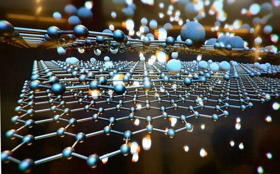
Illustrative introductory photo: Pixabay.com / seagul /
Source: https://vedanadosah.cvtisr.sk/
Posted by: MS