 Contact
 Intranet
 SK
SK


Laboratory provides technology of semiconductor microelectronic structures and devices in using material vacuum deposition, photolithographic operations, and chemical operations.
Equipment:
- TFDS-462B high vacuum deposition equipment (scroll and turbomolecular pump, electron beam evaporation source Telemark TT-6, two thermal evaporation sources 3.2 kW, Telemark 880 thin-film thickness and rate controller)
- UF-30 heating and drying oven (up to temperature 300° C)
- spin coater for application of the photoresist
- one-side optical mask aligner, control optical microscope
- two chemical boxes for the work with organic and inorganic agents
Application:
- high vacuum deposition of metals to make contact layers for semiconductor structures and devices
- photolithographic processing of semiconductor wafers to the 3″ diameter
- cleaning and wet chemical etching of semiconductor wafers
Contact: P. Boháček, Tel.: +421-33-3811406 (deposition equipment)
Access: Place an order
Price: Based on quotation (running costs and consumables)
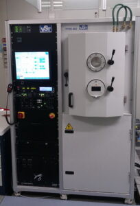
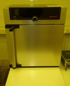
HV deposition system TFDS-462B and heating and drying oven UF-30
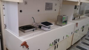
Chemical boxes for inorganic (left) and organic (right) agents