 Contact
 Intranet
 SK
SK


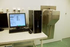
The laboratory provides Inductively-Coupled Plasma Reactive Ion Etching (ICP RIE) of selected materials. Our research is primarily focused on etching of the GaN, AlGaN, InAlN, GaAs and InN semiconductors. The ICP RIE provides high precision etching and low damage selective reactive ion etching (SRIE). A simple vacuum Load‑lock system is suitable for 4‑inch wafers as well as pieces which can be mounted on a handle wafer. ICP RIE equipment is operated by the control computer located in the clean room.
Equipment:
Oxford Plasmalab 100 Inductively Coupled Plasma (ICP) etching system equipped with
- 13,6 MHz supply with automatic matching at the substrate electrode
- 3 kW Inductive Coupled Plasma (ICP 180) Source with electrostatic shielding
- temperature range substrate electrode: -30 + 80°C
- automatic 4-inch/100 mm wafer Load‑lock system
- PC Control with OPT PC2000 RIE Software under Windows 7
Application:
- Etching of semiconductor materials and heterostructures based on GaN, AlGaN, InAlN, GaAs, and InN using the chlorine chemistry or its mixtures with fluorinated compounds
- Etching heterostructure layers (AlGaAs, GaAs, InGaAs, and InP) using SiCl4/Cl2, BCl3/Cl2, and Cl2/Ar
- Etching SiO2, Si3N4 and SiC by the CF4 and SF6 gases
Contact: RNDr. Š. Haščík, PhD., Tel.: 421-2-5941 1272, 421-2-5922 2956
Access: place an order
Price: Based on quotation (running costs and consumables)
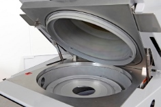
Process chamber capable to accommodate 100 mm/4-inch wafer
Process chamber capable to accommodate 100 mm/4-inch wafer