 Contact
 Intranet
 SK
SK


The laboratory provides complex analysis of physical properties of the surface by means of scanning electron microscopy and scanning probe microscopy. The laboratory allows scientists to image, characterize and even modify material structures in the range of few millimeters down to sub 100-nm scale. The surface modification of samples can be performed by local anodic oxidation or by electron beam lithography.
Equipment:
- NTEGRA Prima, scanning probe microscope (SPM) equipped with complementary probe techniques, including MFM, EFM, KPM and LAO lithography
- Inspect F50, scanning electron microscope equipped with Elphy Quantum lithography control software (Raith) and laser interferometric measuring system for precise stage positioning
- FEG250, scanning electron microscope with resolution of 1.2 nm equipped with SE and BSE detector with possibility to measure in environmental mode (for non-conductive samples)
Application:
- topography imaging of conductive and non-conductive samples
- analysis of surface roughness
- specialized magnetic measurements with external magnetic field up to 200 mT
- local anodic oxidation lithography
- electron-beam lithography
Contact: Ing. J. Šoltýs, PhD., Tel.: +421-2-5922 2652
Access: Guided access or individual access after introductory training (4 – 8 hours)
Price: 0 Eur/hour for SAS employees
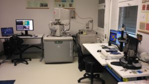
Scanning electron microscope FEG250 (in the middle) with resolution of 1.2 nm and scanning probe microscope NTEGRA Prima (right) with typical resolution of 0.1 nm