 Contact
 Intranet
 SK
SK


- Fabrication and study of few-layer PtSe2 films
M. Sojková, J. Hrdá, T. Vojteková, L. Pribusová Slušná, M. Hulman
Few-layer PtSe2 films are promising candidates for applications in high-speed electronics, spintronics and photodetectors. We reported the fabrication of epitaxially aligned PtSe2 films using one-zone selenization of pre-sputtered platinum layers on the c-plane sapphire substrate. The use of elevated temperature led to enhanced crystallinity and better electrical properties.1 Moreover, we have identified the Se : Pt ratio as a parameter controlling the charge carrier mobility in the films. The mobility increases more than twice as the ratio changes in a narrow interval around a value of 2.2 Combining a semiconductor with a superconductor on a single platform is expected to provide devices with improved performance. we report on the fabrication of a few-layer PtSe2 film on top of an NbN substrate. We found the selenization parameters preserving the chemical and structural integrity of both the PtSe2 and NbN films. The PtSe2 film alignment can be tuned by varying the nitrogen flow rate through the reaction chamber.3
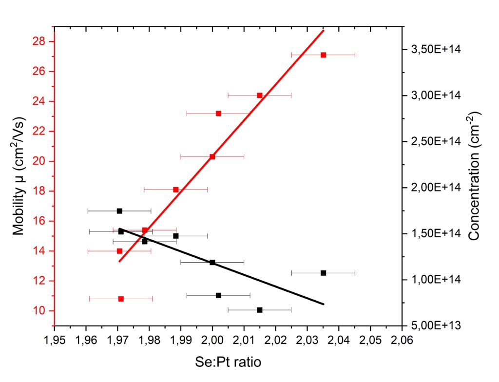
Fig. 1 Se : Pt ratio vs. charge carrier mobility and carrier concentration of PtSe2 films prepared by selenization of 1 nm thick Pt layer at 550 °C during 30 min with different N2 flow rate
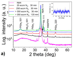
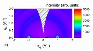
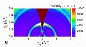
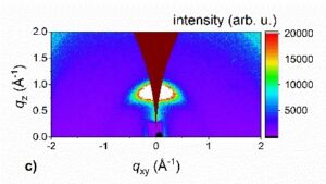
Fig. 2. (a) XRD pattern of NbN substrate layer and PtSe2 films prepared by selenization of 3 nm thick platinum layer at 550 °C on the NbN substrate using different nitrogen flow rates and annealing times. (b) Schematic sketch showing the arrangement of a PtSe2 films on an NbN / sapphire substrate.
Outputs:
Sojková, M., Dobročka, E., Hutár, P., Tašková, V., Pribusová Slušná, L., Stoklas, R., Píš, I., Bondino, F., Munnik, F., and Hulman, M.: High carrier mobility epitaxially aligned PtSe2 films grown by one-zone selenization, Applied Surface Sci 538 (2021) 147936.
Hrdá, J., Tašková, V., Vojteková, T., Pribusová Slušná, L., Dobročka, E., Píš, I., Bondino, F., Hulman, M., and Sojková, M.: Tuning the charge carrier mobility in few-layer PtSe2 films by Se: Pt ratio, RSC Adv. 11 (2021) 27292. (APVV 17-0352, 17-0560, 19-0365, VEGA 2/0059/21, CEMEA ITMS 313021T081)
Sojková, M., Hrdá, J., Volkov, S., Vegso, K., Shaji, A., Vojteková, T., Pribusová Slušná, L., Gál, N., Dobročka, E., Šiffalovič, P., Roch, T., Gregor, M., and Hulman, M.: Growth of PtSe2 few-layer films on NbN superconducting substrate, Applied Phys. Lett. 119 (2021) 013101. ( APVV 15-0693, 17-0352, 297, 17-0560, 19-0365, VEGA 2/0149/17, 2/0059/21, CEMEA ERDF ITMS 313021T081)
- HTS Energy Applications Study
F. Gömöry, T. Kujovič, M. Mošať, R. Ries, E. Seiler, M. Solovyov
GSI Darmstadt and external partners are currently developing a new cable for fast-ramped accelerator magnets. This cable similar to the CORT/CORC design, based on helically arranged coated conductor tapes, shall be operated in the temperature range up to 30 K and carry current up to 30 kA while having an outer dimension in the order of 10 mm. To investigate the use of such a cable in other applications GSI has asked our group to investigate the possibility of using CORT cable in the field of electric power. In the first step we performed thorough literature survey on energy applications of HTS cables irrespective of the cable type [1]. Based on the conclusion of this stage it was decided to eleaborate further the posibility of using CORT conductor in the Resistive Superconducting Fault Curent Limiter. Main advantage of such conductor is its simple adaptability to higher operating currents while keeping uniform the distribution of currents among parallel tapes. As conclusion of this Study the research necessary for developing the concept to the stage of verification in laboratory environment has been formulated [2].
Outputs:
F. Gömöry, T. Kujovič, M. Mošať, R. Ries, E. Seiler: HTS Applications Study: Literature Study, Bratislava, September 2021
F. Gömöry, T. Kujovič, M. Mošať, R. Ries, E. Seiler, M. Solovyov: HTS Applications Study: Superconducting Fault Current Limiter from CORT, Bratislava, December 2021
- Magnetic skyrmions in nanodisks
M. Mruczkiewicz, I.V. Vetrova, J. Šoltýs, T. Šcepka, J. Dérer, R. Stoklas, V. Cambel
Magnetic skyrmions are topologically protected spin textures that currently attract considerable attention in fundamental and applied physics. We observed skyrmions in patterned nanodots fabricated by electron lithography and dry etching. The nanodots were composed of an ultrathin Pt/Co/Au multilayer, exhibiting the interfacial Dzyaloshinskii-Moriya interaction and a perpendicular magnetic anisotropy [1, 2]. In submicrometer dots with a diameter of 150–525 nm, we investigated the stabilization of various magnetic states, such as single-domain states, skyrmionic states, horseshoe-like domain structures, and worm-like domain structures. We have shown that a stack of six repetitions of Pt/Co/Au layers suffices to stabilize the skyrmion state inside a dot at room temperature. We demonstrate the process of skyrmion formation in nanodots by micromagnetic simulations [3]. We have found that the field generated by the sharp magnetic tip significantly affects the magnetization state of the nanodots and leads to the formation of skyrmions. The simulation explains the development of the magnetic state in the dot during magnetic force microscopy scans and confirms the possibility of skyrmion formation. The key transition in this process is the formation of the magnetic horseshoe domain.
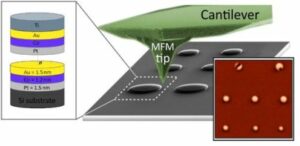
Fig. Schematic representation of multilayer nanodot based on ultrathin Co layers placed between two different heavy metals: Au, Pt (left). An array of multilayer dots is scanned by MFM tip (middle), and its magnetic state is modified during the scan (right).
Outputs:
Vetrova, Iu.V., Zelent, M., Šoltýs, J., Gubanov, V.A., Sadovnikov, A.V., Ščepka, T., Dérer, J., Stoklas, R., Cambel, V., and Mruczkiewicz, M.: Investigation of self-nucleated skyrmion states in the ferromagnetic/nonmagnetic multilayer dot, Applied Phys. Lett. 118 (2021) 212409. (ITMS 313021T081, APVV-16-0068, 19-0311(RSWFA), VEGA 2/0160/19)
Zelent, M., Vetrova, Iu.V., Li, X., Zhou, Y., Šoltýs, J., Gubanov, V.A., Sadovnikov, A.V., Ščepka, T., Dérer, J., Stoklas, R., Cambel, V., and Mruczkiewicz, M.: Skyrmion formation in nanodisks using magnetic force microscopy tip, Nanomater. 11 (2021) 2627. (ERDF 313021T081, APVV 19-0311(RSWFA)), ERA.Net RUS Plus (TSMFA), VEGA 2/0160/19)
Vetrova, Iu.V., Šoltýs, J., Zelent, M., Sadovnikov, A.V., Gubanov, V.A., Ščepka, T., Dérer, J., Stoklas, R., Cambel, V., and Mruczkiewicz, M.: Investigation of the self-nucleated skyrmion states inside the ferromagnetic/non-magnetic multilayer dot. In: Sol-SkyMag 2021, virtual.
- Controlled motion of skyrmions in a magnetic antidot lattice
Feilhauer, S. Saha, J. Tóbik, M. Zelent, L. J. Heyderman, and M. Mruczkiewicz
Magnetic skyrmions are robust defects in the out-of-plane magnetization of thin ferromagnetic layers where they can be moved by applying a spin polarized electric current. Due to the relatively low power required for their manipulation, skyrmions are promising candidates for the information carriers in the future efficient memory-storage devices and logical gates. However, spintronic devices based on skyrmions will require precise control of the skyrmion motion. We show that this goal can be achieved through the use of magnetic antidot array, i.e. square lattice of circular holes patterned in the ferromagnetic layer (see Fig.1). We perform micromagnetic simulations and semi-analytical calculations based on Thiele equation, where the skyrmion motion is driven by applied electric current. We demonstrate that an antidot array can guide the skyrmions in different directions depending on the parameters of the applied current pulse. Despite the fixed direction of the net driving current, due to the non-trivial interplay between the repulsive potential introduced by the antidots, the skyrmion Hall effect and the non-uniform current distribution, full control of skyrmion motion in a 2D lattice can be achieved. Moreover, we demonstrate that the direction of skyrmion motion can be controlled by tuning only a single parameter of the current pulse, i.e. current magnitude (see Fig.2).
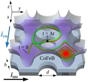
Obr.1: Antidot lattice in the ferromagnet (CoFeB)/ heavy metal (HM) heterostructure with an example of current-driven skyrmion trajectory
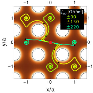
Obr.2: Skyrmion trajectories in the antidot lattice for different magnitudes of applied current pulse
Outputs:
Feilhauer, J., Saha, S., Tóbik, J., Zelent, M., Heyderman, L.J., and Mruczkiewicz, M.: Controlled motion of skyrmions in a magnetic antidot lattice, Phys. Rev. B 102 (2020) 184425. (ERDF ITMS 313021T081, APVV-16-0068, 19-0311, Era.Net RUS Plus (TSMFA), VEGA 2/0162/18, 2/0150/18, UF, NSC, Poland UMO-2017/27/N/ST3/00419, No. UMO2018/30/Q/ST3/00416 and Nat. Scholarship Programme SR)
- Performance of High Temperature Superconducting Tapes
Gömöry, T. Kujovič, M. Mošať, E. Seiler, M. Solovyov, J. Šouc
On request of the particle accelerator facility GSI Darmstadt (Germany) we have carried out the study on a possible use of commercially available conductors, based on the high-temperature superconducting (HTS) compounds manufactured in form of Coated Conductor (CC) tapes, for winding of a coil generating magnetic field pulses of few seconds duration, that could be utilized in a future particle accelerator. Use of HTS in difference to the currently used NbTi cables should allow a significant increase of the operating field thus the accelerator power. Based on our previous experience in characterizing the current transport capability of CC tapes produced by various techniques and the achievements in modelling of a likely mechanical damage during the tape assembling, assessment of possible design options of the Conductor-On-Round-Tube (CORT) cable was accomplished. Finite element computations in the Comsol Multiphysics environment revealed that none of the CC tapes commercially available could comply with the requirements set by the preliminary coil design elaborated at GSI.
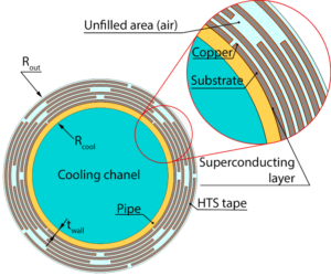
Cross-section of CORT cable used in magnetic field computation. HTS tapes are laid helically in several layers on the central tube serving for the flow of a coolant
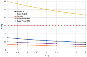
Maximum current transporting capability of four cables designed from the commercially available tapes (SuperOx, SuNAM, SuperPower -two tapes) and the hypothetical tape SuperOx (V2) with radically improved properties. Requirement of the preliminary coil design is marked by the dash-dotted line
Outputs:
Kujovič, T. and Gömöry, F.: Impact of local geometrical irregularities on critical currents of REBCO tapes in round cables, Supercond. Sci Technol. 33 (2020) 115008. (APVV 16-0418)
- Tailored growth of MoS2 few-layer films
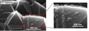
Few-layer MoS2 films are promising candidates for applications in many areas, such as photovoltaics, photocatalysis, nanotribology, lithium batteries, hydrogenation desulfurization catalysis and dry lubricants, mainly due to their characteristic electronic, optical and catalytic properties. In general, two orientation options of the MoS2 layers are possible – horizontal (with the c-axis perpendicular to the plane of the substrate) and vertical (where the c-axis is parallel to the substrate), having different physicochemical properties. In the preparation of these materials by the sulfurization of molybdenum layers, the initial thickness of the molybdenum proved to be a critical parameter affecting the final orientation of the MoS2 layers. Unlike standard CVD chambers, where the reaction takes place in a two-zone furnace, we use a single zone furnace where we have a substrate and sulfur together at a high temperature in the center of the furnace. The aim of the work was to study the influence of other annealing parameters on the orientation of layers. The heating rate has been shown to be a critical parameter for the growth mechanism where rapid sulfurization leads to the growth of vertical MoS2 layers and slow sulfur evaporation leads to horizontal growth even for thicker initial molybdenum layers.
GIWAXS reciprocal space maps of MoS2 films on the c-plane sapphire substrate prepared from 3 nm thick Mo layers at 800 °C during 30 min with the heating rate of (a) 25 °C / min, (b) 5 °C / min and (c) 0.5 °C / min. The peaks at ~ 1 Å-1 originate from the (002) diffraction planes.
In addition, the single-zone sulfurization method used allowed the growth of MoS2 on the surface of the CVD microcrystalline diamond layers. This experimental design results in a sulfur-rich environment during the process, and diffusion of sulfur into molybdenum at temperatures below that required for formation of molybdenum carbide prevents the formation of the latter at the Mo-diamond interface. This finding may open a way for growing MoS2 layers on substrates which are otherwise susceptible to a chemical reaction with molybdenum. We have also shown that horizontal and vertical growth of the MoS2 layers is possible, depending on the thickness of the Mo layer as in the case of unstructured substrates. The combination of unique diamond properties and ultra-thin MoS2 layers with tunable crystallographic orientation can offer material properties relevant to a wide range of applications.
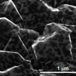
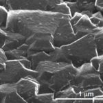
SEM images of MoS2 layers grown from (a) 1 nm, (b) 3 nm and (c,d) 6 nm thick Mo films deposited on the microcrystalline CVD diamond substrate. In (d), standing MoS2 flakes are seen on the edge of a diamond crystallite
Outputs:
Sojková, M., Végso, K., Mrkývkova, N., Hagara, J., Hutár, P., Rosová, A., Čaplovičová, M., Ludacka, U., Skákalová, V., Majková, E., Šiffalovič, P., and Hulman, M.: Tuning the orientation of few-layer MoS2 films using one-zone sulfurization, RSC Adv. 9 (2019) 29645-29651. IF 3.049, Q SJR 1
Sojková, M., Šiffalovič, P., Babchenko, O., Vanko, G., Dobročka, E., Hagara, J., Mrkývková, N., Majková, E., Ižák, T., Kromka, A., and Hulman, M.: Carbide-free one-zone sulfurization method grows thin MoS2 layers on polycrystalline CVD diamond, Sci Rep. 9 (2019) 2001. IF 4.011, Q SJR 1
- Production and delivery of 4H-SiC sensors of ionizing radiation developed for requirement of the laboratory for research purposes
Zaťko, F. Dubecký, P. Boháček, M. Sekáčová, J. Arbet
We developed special large area detector of ionizing radiation. The sensor is based on a 4H-SiC high-quality epitaxial layer. The original contribution is a replacement of one large area detector of 40 mm2 with a foursome’s smaller sensor of 10 mm2 each. The special developed holder allows the selection of connection each sensor individually to the input of readout electronics. This solution provides higher production yield and also lower amount of the noise in case of each detector connection to the individual preamplifier input.

The photo of 4H-SiC sensors of ionizing radiation glued and bonded on the special holder.
- Metadynamics
Knowledge of free energy barriers separating different states is critically important for assessment of long-term stability of information stored in magnetic devices. This information, however, is not directly accessible by standard simulations of microscopic models because of the ubiquitous time-scale problem, related to the fact that the transitions among different free energy minima have character of rare events. Here we show that by employing the metadynamics algorithm based on suitably chosen collective variables, namely helicity and circulation, it is possible to reliably recover the free energy landscape. We demonstrate the effectiveness of the new approach on the example of vortex nucleation process in magnetic nanodot with lowered spatial symmetry. With the help of reconstructed free energy surfaces (FES) we show the origin of the symmetry broken vortex nucleation, where one polarity of the nucleated vortex core is preferred, even though only in-plane magnetic field is present.
Tóbik, J., Martoňák, R., Cambel, V., : Free-energy landscapes in magnetic systems from metadynamics. Phys. Rev. B 96 (2017) 140413(R). (APVV 0088-12, VEGA 2/0180/14, VEGA 2/0200/14).
- Study of surface charges in III-N heterostructures for preparation of GaN power switching devices
Heterostructure field effect transistors (HFET) based on gallium nitride (GaN) represent a new promising technology for high-power and mixed-signal electronics. Despite ongoing industrialization of GaN electronic devices, there is still limited understanding on the formation of GaN surface charges, being vital for the device’s threshold voltage adjustment. Specifically, origin of the oxide/semiconductor interface charges in HFETs with metal-oxide-semiconductor (MOS) gate is still under debate. In our works, we demonstrated several technological approaches to manipulate interface charges in GaN MOS-HFETs with gate dielectrics grown by different deposition techniques. First, we evaluated all relevant charges located at oxide/semiconductor interface that were then correlated with microstructural and chemical properties of the interface. The results show possibilities to manipulate the surface charges and indicate their origin. Such knowladge is unavoidable for development of the next-generation high-power and high-speed GaN transistors.

HRTEM micrograph of Al2O3/AlGAN/GaN structure
Ťapajna, M., Stoklas, R., Gregušová, D., Gucmann, F., Hušeková, K., Haščík, Š., Fröhlich, K., Tóth, L., Pecz, B., Brunner, F., Kuzmík, J., : Investigation of ‘surface donors’ in Al2O3/AlGaN/GaN metal-oxide-semiconductor heterostructures: Correlation of electrical, structural, and chemical properties. Applied Surface Sci 426 (2017) 656-661. (CENTE II, APVV 15-0031, VEGA 2/0138/14).
Ťapajna, M., Válik, L., Gucmann, F., Gregušová, D., Fröhlich, K., Haščík, Š., Dobročka, E., Tóth, L., Pecz, B., Kuzmík, J., : Low-temperature atomic layer deposition-grown Al2O3 gate dielectric for GaN/AlGaN/GaN MOS HEMTs: Impact of deposition conditions on interface state density. J. Vacuum Sci Technol. B 35 (2017) 01A107. (SAFEMOST, VEGA 2/0138/14, CENTE).
- Thermo-mechanical analysis of uncooled La0.67Sr0.33MnO3 microbolometer made on circular SOI membrane
We report on thermal and mechanical analysis of uncooled antenna-coupled La0.67Sr0.33MnO3 microbolometer made on circular SOI (Silicon On Insulator) membrane with no limitation in its active area (circular membrane with diameter up to 2 500 mm). A simple method how to investigate the thermal conversion efficiency (thermal resistance value – Rth) is introduced. Thermal analysis is supported by the ANSYS modelling and simulation. It is found that Rth and thermal time constant (t) of our LSMO microbolometer (bolometer sensitivity and time response) can be tuned by the SOI membrane thickness. Rth value as high as 188 K/mW and t value as low as 0.88 ms are estimated from the thermal simulation for SOI membrane with total thickness of 300 nm (SiO2-200 nm, Si-100 nm). Genesis of the induced mechanical stress changes after main processing steps is found and evaluated to explain the mechanical stability of the LSMO based MEMS microbolometer.
Lalinský, T., Dzuba, J., Vanko, G., Kutiš, V., Paulech, J., Gálik, G., Držík, M., Chromik, Š., and Lobotka, P.:Thermo-mechanical analysis of uncooled La0.67Sr0.33MnO3 microbolometer made on circular SOI membrane. Sensors Actuators A 265 (2017) 321–328. (APVV 14-0613, APVV 0450-10, APVV 0455-12, CENTE II).
- Skyrmion stability in nanodots
In collaboration with Adam Mickiewicz Univeristy in Poznan, Poland and University of the Basque Country, Spain we have studied the stability of skyrmion in nanodots. Magnetic skyrmions are stable, circularly symmetric inhomogeneous magnetization configurations. These topologically protected states of nanometer size have a potential to provide useful solution for low-power, high-density data storage and processing. Typically, ultrathin layers of ferromagnetic and heavy metal layers with various number of repeats are used to stabilize skyrmions in thin films. We have studied influence of confinement, dipole interactions[Zelent 2017] and pinning [Zeissler 2017] on the skyrmion stability. We show how these effects lead to enhancement of skyrmion stability. We have demonstrated, that due to the lateral confinement and strong magnetostatic interactions introduced by multiple repetition of the layers, the two skyrmions of different sizes can stabilize in the same nanodot in dependence on the magnetic reversal history [Zelent2017]. Finally, we have proposed a nanodot with the bi-stable skyrmion states at zero magnetic field, with feasible switching between these two states. Bi-stability was also found experimentally in nanodot and our micromagnetic simulations incorporating disorder were used to explain the hysteresis in skyrmion size [Zeissler]. Our result can open a new route to develop an efficient skyrmion memory, where information would be coded as a skyrmion’s equilibrium size.
Zelent, M., Tóbik, J., Krawczyk, M., Guslienko, K., Mruczkiewicz, M., : Bi‐stability of magnetic skyrmions in ultrathin multilayer nanodots induced by magnetostatic interaction. Physica Status Solidi RRL 11 (2017) 1700259. (SASPRO 1244/02/01).
Zeissler, K., Mruczkiewicz, M., Finizio, S., Raabe, J., Shepley, P., Sadovnikov, A., Nikitov, S., Fallon, K., McFadzean, S., McVitie, S., Moore, T., Burnell, G., Marrows, C., : Pinning and hysteresis in the field dependent diameter evolution of skyrmions in Pt/Co/Ir superlattice stacks. Sci Rep. 7 (2017) 15125.(SASPRO 1244/02/01).