 Contact
 Intranet
 SK
SK


Silicon is not enough anymore. Advanced electronics require more suitable materials
Semiconductors are materials that, from the point of view of electrical conductivity, are between electrically conductive and non-conductive materials. Scientists’ interest in semiconductors increased considerably after the first transistor was created in 1957.
“Today, it is clear to everyone that without semiconductors and complex integrated circuits prepared from them, there would be no modern electronics or the modern electronic devices that almost everyone uses every day. Many of us also know that the most widespread semiconductor material nowadays is silicon,” says RNDr. Dagmar Gregusova, DrSc. from the Institute of Electrical Engineering of the Slovak Academy of Sciences, a principal investigator of the project “Semiconductor Surface Treatment as a way to new III-As and III-N electronic components”.
But the fact is that electronic devices are more and more demanding today and the demands on increasing the speed and volume of transferred data are increasing. The use of silicon thus reaches the edge of its physical limit.

The figure shows a transistor prepared on a sapphire substrate. It consists of a GaN / AlGaN heterostructure and aluminum oxide is deposited on the surface in order to improve the surface properties and thus the output current of the transistor.
New types of compound semiconductors
The increased demands of today’s electronics, therefore, require the selection of more suitable semiconductor material. It is also important to focus on other important material parameters such as frequency, efficiency or resistance to adverse environments (temperature, pressure, radiation).
In this project, scientists from the Institute of Electrical Engineering of the Slovak Academy of Sciences investigate the properties of compound semiconductor surfaces and their impact on the functionality of devices.
“We are investigating new types of compound semiconductors such as gallium arsenide (GaAs) and gallium nitride (GaN) and their ternary compounds, and of course the heterostructures made from these materials. The properties of surfaces and interfaces between individual layers and their influence on the parameters of the device are studied on the prepared electronic components, which in our case are transistors. In addition to electrical measurements, we also use other methods to assess surface quality, to determine bonds between individual elements and surface contamination,“ said the expert.

The aim of the project is to find technological steps that could lead to the elimination of the influence of the surface on the properties of transistors.
“We are investigating the possibilities of semiconductor structures fabrication with the surface having the lowest possible density of the various capture centers, which then impose unwanted charge ratios into the device itself. We also investigate the possibility of surface passivation to cover these charge states with a suitable dielectric layer so that their charge activity is eliminated. Knowing the surface properties and interfaces between the individual semiconductor layers in a heterostructure will allow us to take full advantage of the properties of compound semiconductors and the reliability of electronic systems.” According to her, it is expected that successful manipulation of surface states can lead to the production of new devices, which could lead to the improvement of functionality and more versatile or reliable electronic systems.

The figure shows a detail of the patterned gate-control electrode of the transistor.
Expert guarantor of the text and illustration provided by RNDr. Dagmar Gregušová, DrSc.
Prepared by: Slávka Cigáňová (Habrmanová), NCP VaT at CVTI SR
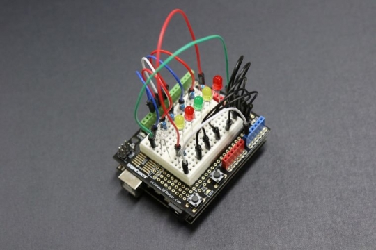
Illustrative introductory photo: Pixabay.com /manseok/
Source: https://vedanadosah.cvtisr.sk/
Posted by: MS