 Contact
 Intranet
 SK
SK


Growth of thin films using pulsed laser deposition (PLD) technique
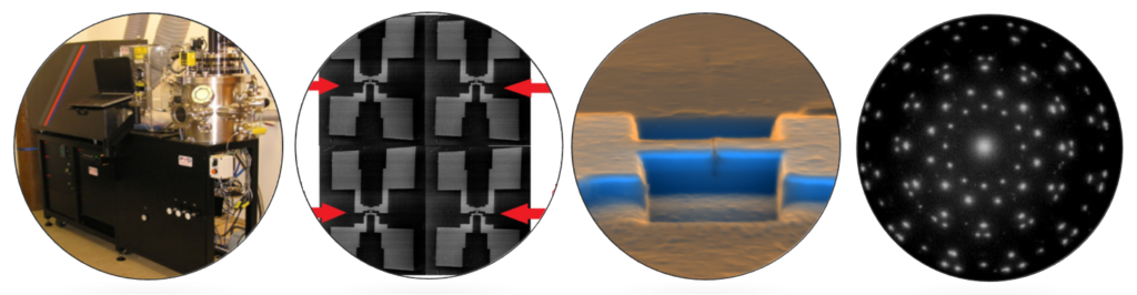
MBE/PLD-2000 system
Pulsed laser deposition is a physical vapor deposition technique where a high-power pulsed laser beam is focused inside a vacuum chamber to strike a target of the material that is to be deposited. This material is vaporized from the target (in a plasma plume) which deposits it as a thin film on a substrate. This process can occur in ultrahigh vacuum or in the presence of a background gas, such as oxygen.
The main advantages of PLD are -conceptually simple (a laser beam vaporizes a target surface, producing a film with the same composition as the target), -versatile (many materials can be deposited in a wide variety of gases over a broad range of gas pressures), -cost-effective (one laser can serve many vacuum systems, the targets used in PLD are small compared with the large size required for other sputtering techniques), -fast (high quality samples can be grown reliably in 10 or 15 minutes). This technique enables to produce multi-layered films and structures in one vacuum cycle. And because of the high heating rate of ablated materials, laser deposition of crystalline film demands lower substrate temperature than other film growth techniques. For this reason the semiconducting and superconducting structures can refrain from thermal degradation.
The equipment is used for the preparation of dielectric (MgO, CeO2, YSZ, SrTiO3, Bi4Ti3O12, BaZrO3, TiO2), perovskite-like superconducting (YBa2Cu3O7-x), manganite (La0.67Sr0.33MnO3) films and structures for possible applications, e.g. bolometer, as well as for the preparation of structures for study of interaction between superconducting and ferromagnetic layers. In recent years, the PLD has also been used to deposit two-dimensional chalcogenide films of MoS2, WS2 and the effect of substrate type on their structural properties.
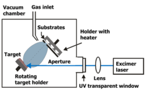
Schematic view of a PLD system
Selected publications:
Španková, M., Chromik, Š., Dobročka, E., Pribusová Slušná, L., Talacko, M., Gregor, M., Pécz, B., Koos, A., Greco, G., Panasci, S.E., Fiorenza, P., Roccaforte, F., Cordier, Y., Frayssinet, E., and Giannazzo, F.: Large-area MoS2 films grown on sapphire and GaN substrates by pulsed laser deposition, Nanomater. 13 (2023) 2837.
Španková, M., Sojková, M., Dobročka, E., Hutár, P., Bodík, M., Munnik, F., Hulman, M., and Chromik, Š.: Influence of precursor thin-film quality on the structural properties of large-area MoS2 films grown by sulfurization of MoO3 on c-sapphire, Applied Surface Sci 540 (2021) 148240.
Rýger, I., Lobotka, P., Steiger, A., Chromik, Š., Lalinský, T., Raida, Z., Pítra, K., Zehetner, J., Španková, M., Gaži, Š., Sojková, M., and Vanko, G.: Uncooled antenna-coupled microbolometer for detection of terahertz radiation, J. Infrared, Millimet., Terahertz Waves 42 (2021) 462–478.
Bareli, G., Chromik, Š., Camerlingo, C., Talacko, M., Rosová, A., Španková, M., Štrbik, V., Sojková, M., and Jung, G.: Substrate influence on low energy electron beam processing of YBa2Cu3O7−δ thin films, Applied Surface Sci 535 (2021) 147624.